- 您现在的位置:买卖IC网 > Sheet目录320 > DK-DEV-4SE530N (Altera)KIT DEV STRATIX IV FPGA 4SE530
�� �
�
�4–6�
�c�
�Chapter� 4:� Development� Board� Setup�
�Factory� Default� Switch� Settings�
�Installing� shunts� in� certain� configurations� might� cause� damage� to� devices�
�on� your� board.� Pay� specific� attention� to� the� Function� column� details.�
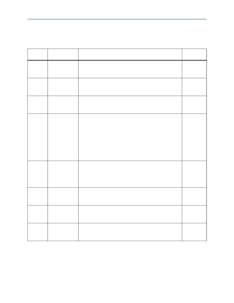
�Table� 4–4.� Jumper� Settings� (Part� 1� of� 2)�
�Board�
�Reference�
�Board�
�Label�
�Function�
�Default�
�Shunt� Position�
�This� jumper� has� the� following� options:�
�J2�
�MSEL0�
�■�
�Installing� the� shunt� sets� MSEL0� to� logic� 0.�
�Installed�
�■�
�Removing� the� shunt� sets� MSEL0� to� logic� 1.�
�This� jumper� has� the� following� options:�
�J4�
�USB� DISABLE�
�■�
�Installing� the� shunt� disables� the� onboard� USB-Blaster.�
�Not� installed�
�■�
�Removing� the� shunt� enables� the� onboard� USB-Blaster.�
�This� jumper� has� the� following� options:�
�J5�
�HSMB_JTAG_EN�
�■�
�Installing� the� shunt� includes� HSMC� port� B� in� the� JTAG� chain.�
�Not� installed�
�■�
�Removing� the� shunt� removes� HSMC� port� B� from� the� JTAG� chain.�
�This� jumper� has� the� following� options:�
�■�
�Installing� the� shunt� on� pins� 1� and� 2� sets� the� QDR� II� output�
�impedance� to� the� minimum� value� possible.�
�J7�
�QDRII� DRIVE�
�■�
�Installing� the� shunt� on� pins� 3� and� 4� sets� the� QDR� II� output�
�impedance� to� 50� Ω� .�
�Installed� on�
�pins� 3� and� 4�
�■�
�Installing� the� shunt� on� pins� 5� and� 6� sets� the� QDR� II� output�
�impedance� to� 60� Ω� .�
�Always� keep� one� and� only� one� shunt� installed.� Other� configurations�
�might� cause� damage� to� the� device.�
�This� jumper� has� the� following� options:�
�■�
�Installing� the� shunt� includes� the� MAX� II� EMP2210� device� in� the�
�J10�
�MAXII_JTAG_EN�
�■�
�JTAG� chain.�
�Removing� the� shunt� removes� the� MAX� II� device� from� the� JTAG�
�Installed�
�chain.�
�This� jumper� has� the� following� options:�
�J11�
�SHUNT=1.8V� QDR�
�■�
�Installing� the� shunt� sets� QDR� II� VDDQ� to� 1.8� V.�
�Not� installed�
�■�
�Removing� the� shunt� sets� QDR� II� VDDQ� to� 1.5� V.�
�This� jumper� has� the� following� options:�
�J15�
�HSMA_JTAG_EN�
�■�
�Installing� the� shunt� includes� HSMC� port� A� in� the� JTAG� chain.�
�Not� installed�
�■�
�Removing� the� shunt� removes� HSMC� port� A� from� the� JTAG� chain.�
�This� jumper� has� the� following� options:�
�J18�
�SHUNT=1.8V� RLD�
�■�
�Installing� the� shunt� sets� RLDRAM� II� VDDQ� to� 1.8� V.�
�Not� installed�
�■�
�Stratix� IV� E� FPGA� Development� Kit� User� Guide�
�Removing� the� shunt� sets� RLDRAM� II� VDDQ� to� 1.5� V.�
�June� 2011� Altera� Corporation�
�发布紧急采购,3分钟左右您将得到回复。
相关PDF资料
DK-DEV-4SGX530N
KIT DEVELOPMENT STRATIX IV
DK-DEV-5AGXB3N/ES
ARRIA V DEVELOPMENT KIT
DK-DEV-5M570ZN
KIT DEV MAX V 5M570Z
DK-DEV-5SGXEA7N
KIT DEV STRATIX V FPGA 5SGXEA7
DK-DSP-2S180N
DSP PRO KIT W/SII EP2S180N
DK-DSP-3C120N
KIT DEV DSP CYCLONE III EDITION
DK-K7-CONN-CES-G
KINTEX-7 FPGA CONNECTIVITY KIT
DK-K7-EMBD-CES-G-J
KINTEX-7 FPGA EMBEDDED KIT JAPAN
相关代理商/技术参数
DK-DEV-4SGX230N
功能描述:可编程逻辑 IC 开发工具 FPGA Development Kit For EP4SGX230KF40C2N
RoHS:否 制造商:Altera Corporation 产品:Development Kits 类型:FPGA 工具用于评估:5CEFA7F3 接口类型: 工作电源电压:
DK-DEV-4SGX230N/C2
功能描述:EP4SGX230KF40C2N Stratix? IV GX FPGA Evaluation Board 制造商:altera 系列:Stratix? IV GX 零件状态:过期 类型:FPGA 配套使用产品/相关产品:EP4SGX230KF40C2N 内容:板,线缆,电源 标准包装:1
DK-DEV-4SGX530N
功能描述:可编程逻辑 IC 开发工具 FPGA Development Kit For EP4SGX530
RoHS:否 制造商:Altera Corporation 产品:Development Kits 类型:FPGA 工具用于评估:5CEFA7F3 接口类型: 工作电源电压:
DK-DEV-5AGTD7N
功能描述:可编程逻辑 IC 开发工具 FPGA Development Kit For 5AGTD7K3F40I3N
RoHS:否 制造商:Altera Corporation 产品:Development Kits 类型:FPGA 工具用于评估:5CEFA7F3 接口类型: 工作电源电压:
DK-DEV-5AGXB3N/ES
功能描述:可编程逻辑 IC 开发工具 FPGA Development Kit For 5AGXFB3H6F ES RoHS:否 制造商:Altera Corporation 产品:Development Kits 类型:FPGA 工具用于评估:5CEFA7F3 接口类型: 工作电源电压:
DK-DEV-5ASTD5N
功能描述:KIT DEV ARRIA V FPGA 制造商:altera 系列:Arria V ST 零件状态:在售 类型:FPGA 配套使用产品/相关产品:Arria? V ST 内容:板 标准包装:1
DK-DEV-5CEA7N
功能描述:可编程逻辑 IC 开发工具 FPGA Development Kit For 5CEFA7F31C7N
RoHS:否 制造商:Altera Corporation 产品:Development Kits 类型:FPGA 工具用于评估:5CEFA7F3 接口类型: 工作电源电压:
DK-DEV-5CEA7N/P
制造商:Altera Corporation 功能描述:Cyclone VE Devkit Promotional 制造商:Altera 功能描述:Cyclone VE Devkit Promotional